
Standard PCB Thickness – It may not be what you think !
The word “thickness” is being used so you can guess what we are talking about, but “WHY IS THE THICKNESS SO IMPORTANT?” well the thickness of a Printed Circuit Board (PCB) affects a lot including its functionality, conductivity and Heat resistivity.
Simply put, the thickness is an essential factor that determines where and how the PCB is applied. Most time, Customers have to define what/where the PCB is to be used, I know that’s elementary, but you can’t generalize with a PCB.
As each design has its preferred thickness and functionality level, so knowing some knowledge about PCB thickness and knowing how to select the thickness of your PCB design is essential. Let’s get the start of reading this article:
- Standard PCB Thickness
- Standard PCB Thickness Fr-4
- Standard PCB Core Thickness
- Standard 2 Layer PCB Thickness
- PCB Thickness Tolerance
- Conclusion
1、Standard PCB Thickness
When we say Standard, we are talking about the first PCBs that were simple in design with a single sided board that had various layers stacked. It refers to the arrangement of single or multiple cores connected with sheets of cured epoxy.
Generally, with PCB thickness, the application or usage area determines how thick the board will be. It is essential during manufacturing of your board; you communicate your specifications like what thickness you would like with your manufacturer.
The thickness ranges from 0.008 inches to 0.240 inches, there are thin Layer PCBs, but the standard or industrial standard PCB thickness is 0.063inches (1.57mm). There is the historical explanation for that specific size, in the beginning; with the development of Circuit Boards which were made of Bakelite sheets.
In the past, Bakelite was thin insulating material that is a good, sturdy insulator that used to be produced in mass numbers of 0.063 inches thickness then were bought and cut to any other specification based on the electronic device.
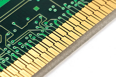
The thickness became an essential part of the circuit board when multiple layer Electronic boards started to emerge. With the multiple layers, the need for a mode of connection between layers was evident, and copper was used for that on the plate edges.
The thickness of the connectors between the boards had to match, and that became the standard PCB THICKNESS.
1.1 PCB Board Thickness
The board thickness is always based on both the insulating material and the top layer material; at the beginning of Circuit boards, this would be Bakelite sheet included as the top layer of the plywood at the end the total thickness of the board would lead to 0.065inches.
Apparently, better substrate like epoxy (fiberglass) with a copper foil bonded on each side or Paper reinforced phenolic resin with a bonded copper foil have been found, making Bakelite plywood almost extinct, with the new lighter materials coupled with the fact that edge connectors are not in use anymore, the thickness sometimes is lesser than the standard 0.065inches.
The PCB created is determined by its size and thickness with most electronic components, devices, and platforms being having a standard PCB thickness.
1.2 PCB Copper Thickness
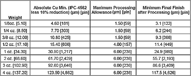
You might think how much of a difference does the copper thickness make and the answer is a lot, as the copper thickness determines the PCBs range of application and functionality.
The Copper thickness plays a vital role on how you select a PCB thickness with the copper thickness measured in ounce per area square foot.
Usually, the Printed Circuit Board is around 1 oz with 1.4 mm to 2.8mm thickness for the internal layer, at the end; the finished weight would be about 2 oz to 3oz which can be adjusted based on your preference.
1.3 PCB Trace Thickness
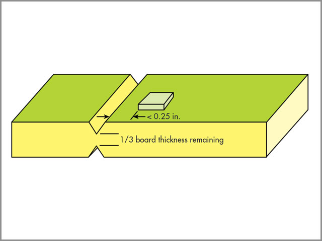
When you talking about Trace thickness of a PCB board, you are talking about the preferable thickness decided by the designer during the design process, the most used trace thickness ranges from 0.008 inches to 0.240 inches with particular attention paid to 0.2 mm (0.0079 inch), 0.4 mm (0.016 inch), 0.5 mm (0.020 inch), 0.6 mm (0.024 inch), 0.8 mm (0.032 inch), 1.0 mm (0.04 inch), 1.2 mm (0.047 inch), 1.5 mm (0.062 inch), 1.6 mm (0.063 inch), 2.0 mm (0.079 inch), 2.3 mm (0.091 inch), etc. when designing Multiple layer boards of 4 or more layers, the user can choose ½, 1 or 2 ounce inner layer copper foil for his board.
In fact, PCB trace thickness calculators are available to the designers to calculate the thickness of the PCB board immediately. In case of wrongly calculating the PCB trace thickness, this may result in either not gaining the accurate results that the PCB designed for or it may also result in damaging the components attached to the surface of the PCB board.
2、Standard PCB Thickness Fr-4
By now, I am sure you have heard a lot about FR-4 (Flame Retardant 4), FR-4 or FR4 is the first material on the shelf when a rigid circuit Board is needed.
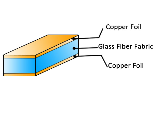
FR4 which also stands for a rating, it is the fiberglass reinforced epoxy-laminated sheets common found in PCB manufacturing. The name also is the base quality rating of the epoxy laminate sheets.
While FR4 has as many as four different materials, the primary material is fiberglass woven into a thin cloth sheet. This gives the low structural stability then it is cover and wrapped with a flame resistant epoxy resin that adds its rigidity (one of its primary quality).
All these qualities make FR4 the first choice for High-Quality, Low-Cost PCBs manufacturing. During manufacturing, the FR4 is joined with one or more layers on both sides of Copper foil using adhesive and heat.
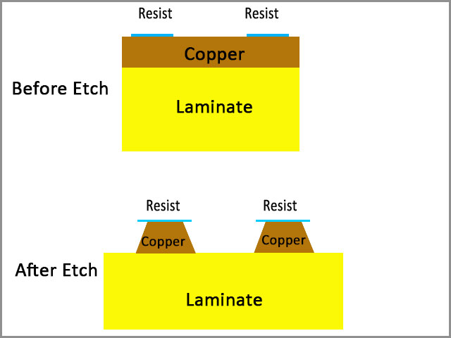
The customer product at the end comes with the copper forming the circuit then they are etched out before the solder mask layer and silkscreen are prepared on the board.
As with every other aspect of a circuit board, the FR4 standard PCB thickness is measured in inches or mm depending on the preference of the designer or manufacturer.
But with the commonness of the FR4 substrate, the thickness of the board tends to go the extremes, you can get from ten thou to three inches.
Sometimes a thin layer is needed and/or best suited for a device, but you are not sure how a small board would take the load, so you go for the standard PCB thickness.
With these extremities, several factors are looked out during the PCBs board design, which includes the following:
• Component Compatibility: we have been talking about how FR4 can be used for any and every PCB. But the fact is The thickness of a board will always affect the components compatibility, this holds true with through-hole components while most components have small board thicknesses.
• Design Requirements: Manufacturers tend to go thicker because there are more downsides to thinner boards on PCBs. With FR4, thinner boards are prone to fractures especially when they are too large and can’t have grooves feature. However, thicker boards do both with flying colors, so you always have to put the weighing options into consideration
• Flexibility: Yes when you have thinner boards, you get a degree of flexibility which is a good thing in some situations or applications like the ECU (Electronic Control Unit) in your Automotive use or in the medical field where you continuously encounter stress and flex to the PCBs.
But at the same time, can be a negative in PCB manufacturing, especially in later processes when the soldering machine wants to solder.
The flexible board might bend during the soldering process causing the components to be soldered at a wrong angle, and also the components and connections can break off the board due to the board’s flexibility.
• Space: you always need to consider space as a factor when designing a PCB especially when you manufacturing small devices like USB connectors and Bluetooth Accessories. Thinner boards are preferred when you need space always.
• Impedance Matching: the thickness of board matters in the case of multilayer boards because the layers are used as capacitors on adjacent layers, and the thickness of the FR4 equals the dielectric thickness and in turn changes the capacitances value.
It is more exact in high-frequency PCBs like your ‘microwave, because without impedance matching. Adequate board functionality is almost zero so there is a crucial need for the capacitance on each layer to be just right.
• Connections: one of the significant factors that affect the customer’s envisioned size in a two-sided PCB design is the edge connector. Because there is always the chance for PCB damage if the mating portion of the connector doesn’t fit correctly on the side of the PCB.
That is primarily why the materials used for the PCB are chosen after the Circuit designs.
Weight: the thickness of the board will always affect the weight of the PCB, in most cases, the weight of the board can be ignored but in consumer electronics is considered as the lighter the board, the lighter the product which in turn means cheaper shipping.
3、Standard PCB Core Thickness
When we are talking about core thickness, we are talking about a layer of FR4 with copper on either side that are manufactured in a core factory. Smooth Copper foils with specific thickness are used to form the layer of FR4.
With Core thickness you have to also look at Pre-preg, this is a fiber weave impregnated with a resin bonding agent made by PCB manufacturers to stick together etched cores. Pre-preg is a thin layer of uncured FR4 that varies with the height of the etched boards either side of it.
The Core is thick fiberglass known for its layer rigidity while the Pre-preg is a thin layer of fiberglass that is used to laminate the core.
When it comes to choosing PCB core thickness, the problem when receiving a request for Multilayer Design PCBs is that it’s never actually stated the material requirements or just partly stated leading to a downgrade in performance.
When the thickness requirement is not met, the customer may not notice it as long as the PCB board works “fine” as the PCB core materials used may not be critical to performance.
PCBs of now though, have performance has an important factor, and the thickness always needs to be precise for the best possible functionality of the board, so the designer always needs to communicate the precise requirements to the fabricator in proper documentation.
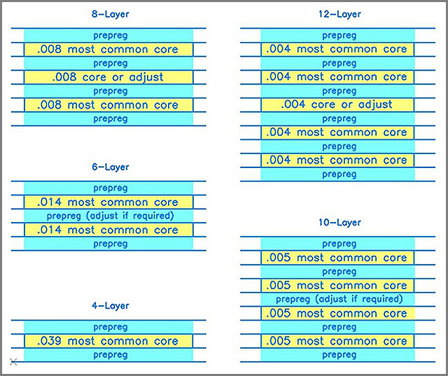
The most common core thicknesses used in multilayer constructions are 0.005″, 0.008″, 0.014″, 0.021, 0.028″, and 0.039″. The 0.047″ is sometimes used when building boards of double layers
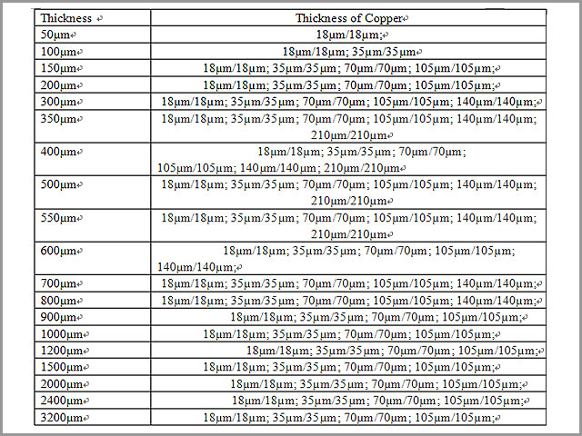
We all know that the copper thickness ranges for half an ounce to 3 ounces based on requirements, keeping in mind that the core layer uses the same copper weight on both sides.
So you always have to avoid using different copper weight on either side of the board during the design phase as that still leads to extra charges.
If you can have a core thickness with a suitable copper weight, you can use some Pre-preg sheets in dielectric positions to meet your overall thickness.
Note that the design phase does not need impedance control so leaving the choice of Pre-preg is advisable as they would use their standard builds but if you do have an impedance requirement in mind, you can always state it on your documentation and the manufacturers will change the Pre-preg between the cores.
The PCB cores have a specific pattern that they follow: Copper foil – Pre-preg – Copper foil and they are always pre-pressed layers.
Reference from: https://www.multi-circuit-boards.eu/en/pcb-design-aid/layer-buildup/prepreg-core-foil.html
4、Standard 2 Layer PCB Thickness
With the advancement in Technology, Multiple Board layers became a thing as the layers allowed for more loads all while still retaining a thickness of 63mm.
Since the layer counts for the PCBs were increased to match up to the wiring requirements of the more complex circuits, the circuit boards were also produced to have a higher layer counts.
That brought about the jump from the standard PCB thickness of 63mils to 93mils. However, with high-temperature materials, Isola’s 370HR can be used in scores of 8, 10, 14, 22 or 39mils respectively.
In other words, the standard PCB thickness depends on the layers of your foil lamination. If the foil lamination is for a four-layer PCB, the standard to be used should be .031+/-10%.
For a six-layer foil lamination, the best standard to be used should be .062+/-10% or .031+/-10% respectively. For 8 and ten layer boards, the standard PCB thickness is at 0.062, 0.093 and 0.125 inches.
4.1 Standard 2 Layer Thickness
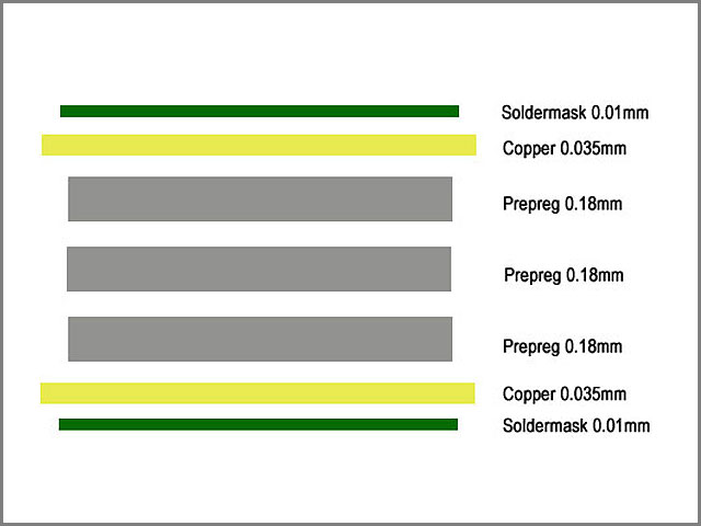
4.2 Standard 4 Layer Thickness
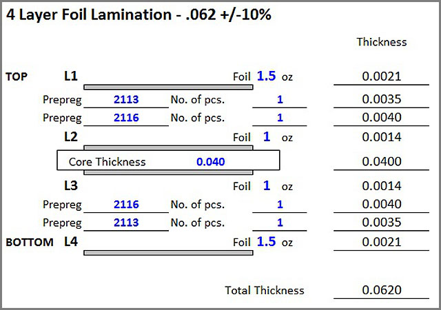
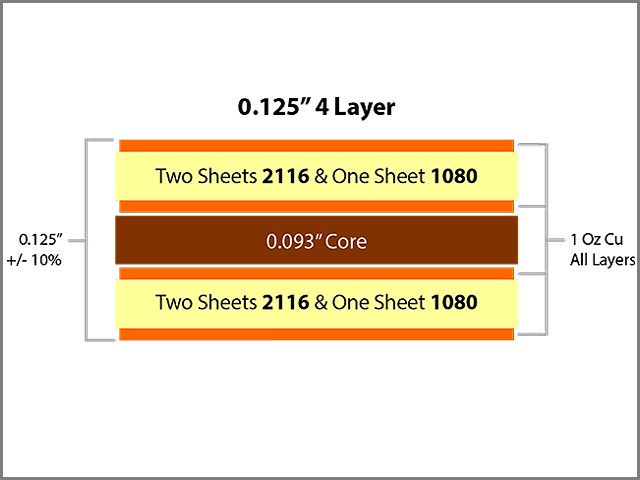
5、PCB Thickness Tolerance
When you are talking about tolerance, you just saying the permitted less or more of a substance and in this case, we say the PCB thickness Tolerance is the permitted less or more thickness that can be allowed by the manufacturers.
There are valid IPC guideline and standards used during manufacturing of a Printed Circuit Boards; it is with these guidelines and rules that a different technical specification was created with smaller tolerance.
Vias Cu Thickness
| Type of Via | Standard Second Class | Third Class |
| Via (>150µm) | 20µm – 25µm max | 20 µm-25 µm max |
| Microvia(<150µm) | 18 µm-20 µm max | 20 µm-25 µm max |
| Blind Via | 10 µm-12 µm max | 10 µm-12 µm max |
| Buried Via | 10 µm-12 µm max | 10 µm-12 µm |
Rigid PCB Base Material
| Type | Tolerance |
| The thickness of Base Material | ± 10% |
Flexible PCB Base Material
| Type | Tolerance |
| The thickness of Dielectric ≥ 0.075mm | ±10 % |
| 0.025mm≤ Thickness of Dielectric ≥ 0.075mm | ± 10% |
| 0.020mm≤ Thickness of Dielectric ≥ 0.075mm | ± 12.5% |
| Thickness of Dielectric < 0.020mm | ± 15% |
| The thickness of adhesive ≥ 0.075mm | ± 10% |
| 0.025mm ≤ Thickness of adhesive ≥ 0.075mm | ± 15% |
| 0.020mm ≤ Thickness of adhesive ≥ 0.075mm | ± 20% |
| The thickness of adhesive < 0.020mm | ± 30% |
| The thickness of adhesive ≥ 0.025mm (this is based on the addition of woven stiffener) | ± 20% |
The Thickness Of Rigid PCB
| Type | Tolerance |
| Standard Level B type of Producibility | ± 10% or ± 178 µm of the higher value |
The Thickness Of Flexible PCB
| Type | Tolerance |
| The thickness of the Flexible Part | ±50 µm |
| The thickness of the Flexible Part and Stiffener | ±100 µm |
6、Conclusion
The significance of PCB thickness is equivalent if not less than that of a PCB board. The PCB thickness holds of immense importance. The designers perform a lot of complex calculations to reach the depth of the PCB board that could deliver accurate results.
So as much as we have talked up how easy it is to design and how the materials are ready, it still takes skilled hands to bring the best PCB for the Customer, and that is us at Ourpcb

